      |


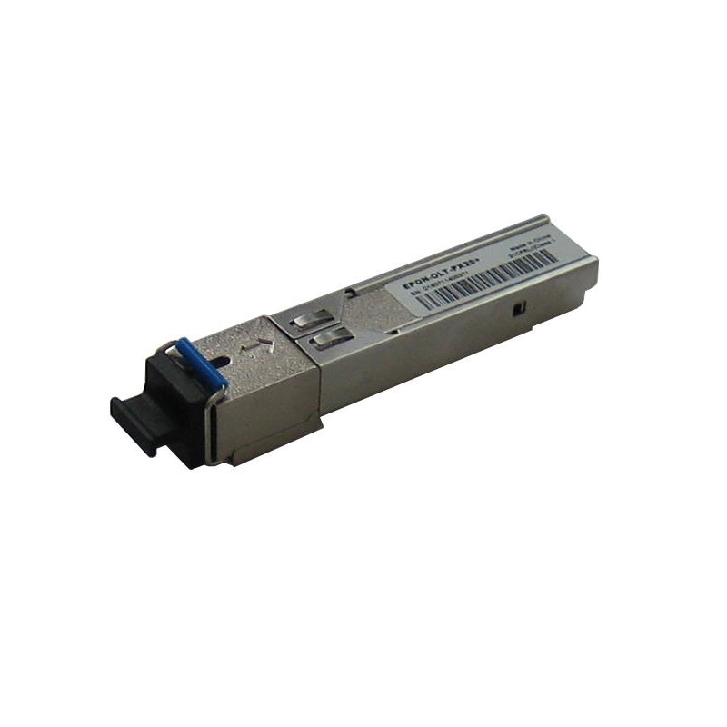
WDS5441H-C(H)3AL is a high performance transceiver module for single fiber communications using a 1490nm continuous-mode transmitter and a 1310nm burst-mode receiver. It is designed to meet CTC 3.0 and IEEE802.3ah -2004 1000BASE- PX20+ applications. Symetric datatransfer with 1,25Gbps speed upstream and 1,25Gbps downstream for up to 20km distance.
The transmitter has automatic power control (APC) function and temperature compensation circuitry to ensure stable optical power output and extinction ratio over all operating temperature range. The transmitter meets Class 1 eye safety per IEC825 and CDRH standards.

Security policy

Delivery policy

Return policy
GEPON OLT SFP Transceiver, 1000BASE-PX20+, for Wodaplug GEPON OLTs
WDS5441H-C(H)3AL is a high performance transceiver module for single fiber communications using a 1490nm continuous-mode transmitter and a 1310nm burst-mode receiver. It is designed to meet CTC 3.0 and IEEE802.3ah -2004 1000BASE- PX20+ applications. Symetric datatransfer with 1,25Gbps speed upstream and 1,25Gbps downstream for up to 20km distance.
The transmitter has automatic power control (APC) function and temperature compensation circuitry to ensure stable optical power output and extinction ratio over all operating temperature range. The transmitter meets Class 1 eye safety per IEC825 and CDRH standards.
The receiver has a hermetically packaged APD-TIA (trans-impedance amplifier) pre-amplifier and a limiting amplifier with LVPECL compatible differential outputs. It features a burst-mode Loss of signal (LOS) output which is LVTTL compatible. The receiver offers bust-mode RSSI outputs, which is I2C
accessible digitized data stored in the internal flash memory.
The module provides digital diagnostic information of its operating conditions and status, including transmitting power, laser bias current, module temperature, supply voltage, and burst-mode receiving power. Calibration and alarm/warning threshold data are written and stored in the internal memory (EEPROM). The memory map is compatible with SFF-8472.
z Single fiber bi-directional data links application with 1.25Gbps upstream and 1.25Gbps downstream. z 1490nm continuous mode DFB transmitter.
z 1310nm burst mode APD-TIA receiver. z High power 1550nm video signal rejection . z 0 to 70°C and -40 to 85°C operating case temperature. z SFP package with SC/UPC receptacle. z Single +3.3V power supply. z LVPECL interface logic level for data input and output. z LVTTL transmitter disable control
z LVTTL transmitter laser failure alarm z LVTTL receiver Loss of Signal (LOS) indication z LVTTL RSSI Trigger control z Low EMI and excellent ESD protection z ClassⅠlaser safety standard IEC-60825 compliant z Complies with RoHS-6
Applications
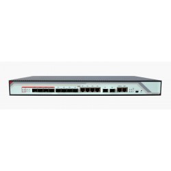
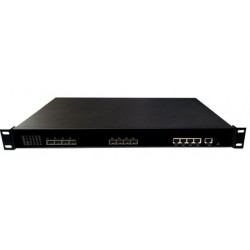
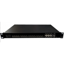
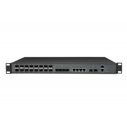
z Gigabit Ethernet Passive Optical Networks(GEPON) – OLT side
z Compliant with SFF MSA - 2000
z Compliant with SFF-8472 Rev.11.0
z Compliant with IEEE 802.3ah-2004
z Compliant with FCC 47 CFR Part 15, Class B
z Compliant with FDA 21 CFR 1040.10 and 1040.11, ClassⅠ
z Complies with China Telecom EPON equipment technology requirement V3.0
|
Parameter |
Symbol |
Minim |
Maxim |
Unit |
Note |
|
Storage Ambient Temperature |
TSTG |
-40 |
85 |
°C |
|
|
Operating Case Temperature |
Tc |
-10 |
75 |
°C |
C-Temp |
|
Operating Case Temperature |
Tc |
-40 |
90 |
°C |
I-Temp |
|
Operating Humidity |
OH |
5 |
95 |
% |
|
|
Power Supply Voltage |
VCC |
0 |
4 |
V |
|
|
Receiver Damaged Threshold |
|
|
4 |
dBm |
|
|
Soldering Temperature |
|
|
260/10 |
°C/S |
|
|
Parameter |
Symbol |
Minim |
Typical |
Maxim |
Unit |
Note |
|
Power Supply Voltage |
VCC |
3.13 |
3.3 |
3.47 |
V |
3.3V±5% |
|
Parameter |
Symbol |
Minim |
Typical |
Maxim |
Unit |
Note |
|
Operating Current |
Icc |
|
|
400 |
mA |
|
|
Operating Case Temperature |
Tc |
0 |
|
70 |
°C |
C-Temp |
|
Operating Case Temperature |
Tc |
-40 |
|
85 |
°C |
I-Temp |
|
Operating Humidity Range |
OH |
5 |
|
85 |
% |
|
|
Data Rate upstream |
|
|
1.25 |
|
Gbit/s |
|
|
Data Rate downstream |
|
|
1.25 |
|
Gbit/s |
|
|
Data Rate Drift |
|
-100 |
|
+100 |
PPM |
|
|
Parameter |
Symb |
Minum |
Typical |
Maxim |
Unit |
Note |
|
Optical Center Wavelength |
λC |
1480 |
1490 |
1500 |
nm |
|
|
Side Mode Suppression Ratio |
SMSR |
30 |
|
|
dB |
|
|
Optical Spectrum Width |
∆λ |
|
|
1 |
nm |
|
|
Average Launch Optical Power |
Po |
+2.5 |
|
+7 |
dBm |
1 |
|
Power-OFF Transmitter Optical Power |
Poff |
|
|
-41 |
dBm |
|
|
Extinction Ratio |
ER |
9 |
|
|
dB |
2 |
|
Rise/Fall Time (20%-80%) |
TR/TF |
|
|
260 |
ps |
2,3 |
|
Optical Return Loss Tolerance |
|
|
|
15 |
dB |
|
|
Transmitter Reflectance |
|
|
|
-10 |
dB |
|
|
Transmitter and Dispersion Penalty |
TDP |
|
|
2.3 |
dB |
4 |
|
Optical Waveform Diagram |
Compliant With IEEE Std 802.3ah™ -2004 Figure 60-6 |
|||||
|
Data Input Differential Swing |
Vinp-p |
200 |
|
2400 |
mV |
5 |
|
Input Differential Impedance |
Zin |
90 |
100 |
110 |
Ω |
|
|
Transmitter Fault Indication Voltage-Low |
VTx_F-L |
|
|
0.4 |
V |
|
|
Transmitter Fault Indication Voltage-Hight |
VTx_F-H |
2.4 |
|
|
V |
|
|
Transmitter enable control Voltage - Low |
Ven-L |
0 |
|
0.8 |
V |
|
|
Transmitter disable control Voltage - High |
Vdis-H |
2.0 |
|
VCC |
V |
|
|
TX Disable Negate time |
Tx_on |
|
|
1 |
ms |
6 |
|
TX Disable Assert time |
Tx_off |
|
|
10 |
us |
6 |
Note 1: Launched into 9/125um Single Mode Fiber.
Note 2: Measured with PRBS 27-1 test pattern @1.25Gbit/s.
Note 3: Measured with the Bessel-Thompson filter OFF.
Note 4: Maximum sensitivity penalty due to transmitter and dispersion effect through 20km of SMF optical fiber.
Note 5: Compatible with LVPECL input, AC coupled internally.
Note 6: Transmitter enable and disable timing
|
Parameter |
Symbol |
Minum |
Typical |
Maxim |
Unit |
Notes |
|
Operating Wavelength |
λC |
1260 |
1310 |
1360 |
nm |
|
|
Sensitivity |
SEN |
|
|
-30 |
dBm |
1 |
|
Saturation Optical Power |
SAT |
-6 |
|
|
dBm |
|
|
Receiver burst_mode dynamic |
|
15 |
|
|
dB |
2 |
|
Burst LOS Assert |
LOSL-H |
-45 |
|
|
dBm |
3 |
|
Burst LOS De-assert Level |
LOSH-L |
|
|
-31 |
dBm |
|
|
Burst LOS Assert time |
TLOSA |
|
|
500 |
ns |
Figure 2 |
|
Burst LOS Deassert time |
TLOSD |
|
|
500 |
ns |
|
|
Receiver Reflectance |
|
|
|
-20 |
dB |
@1310nm |
|
Data Output Voltage-High |
Vout_H |
Vcc-1085 |
|
Vcc-880 |
mV |
4 |
|
Data Output Voltage-Low |
Vout_L |
Vcc-1830 |
|
Vcc-1620 |
mV |
|
|
LOS Voltage - Low |
LOS_L |
0 |
|
0.4 |
V |
|
|
LOS Voltage - High |
LOS_H |
2.4 |
|
VCC |
V |
|
|
RSSI accuracy |
|
-3 |
|
+3 |
dB |
5 |
Note 1: Measured with a PRBS 27-1 test pattern @1.25Gbit/s and ER=10dB, BER =10-12.
Note 2: Input optical power level difference of adjacent burst packets.
Note 3: Low level indicates that burst packet is detected by the receiver.
Note 4: LVPECL output, DC coupled internally, guaranteed in the full range of input optical power (-6dBm
to -30dBm)
Note 5: RSSI DDM accuracy is better than +/-2dB (25℃) or +/-3dB (0℃~70℃) for input power levels between -6 to -30 dBm. Measured with 1310nm, 1.25Gbps PRBS27-1 burst-mode optical input, ER=10dB, 50%duty cycle.
Figure 3 RSSI vs Trigger timing
|
Parameter |
Symbol |
Minum |
Typical |
Maxim |
Unit |
Note |
|
ONT signal width |
Tont |
1000 |
|
|
ns |
|
|
Trigger Delay |
TTD |
|
500 |
|
ns |
|
|
Trigger width |
TTW |
|
500 |
|
ns |
|
|
Time for Sample and IIC time |
TS |
|
500 |
|
µs |
|
|
Parameter |
Accuracy |
Calibration |
Notes |
|
Temp report |
±3℃ |
Internal |
Case Temp ±3℃ |
|
Voltage report |
±3% |
Internal |
Vcc=3.13~3.47V |
|
Ibias report |
±10% |
Internal |
|
|
Optical power output report |
±2dB |
Internal |
Average power |
|
RSSI |
±3dB |
Internal |
Input power levels between -6 to -30 dBm |
|
PIN |
Name |
Description |
Notes |
|
1 |
VeeT |
Transmitter Ground |
|
|
2 |
TX Fault |
Transmitter Fault indication |
Note 1 |
|
3 |
TX Disable |
Transmitter Disable |
Note 2 |
|
4 |
SDA |
I2C data line |
Note 3 |
|
5 |
SCL |
I2C clock line |
Note 3 |
|
6 |
MOD-DEF0 |
Module Definition0 |
Note 3, internal grounded |
|
7 |
RSSI Trigger |
Receiver reset |
Note 4 |
|
8 |
LOS |
Loss of Signal |
Note 5 |
|
9 |
VeeR |
Receiver Ground |
|
|
10 |
VeeR |
Receiver Ground |
|
|
11 |
VeeR |
Receiver Ground |
|
|
12 |
RD- |
Inv.Receiver Data Out |
Note 6 |
|
13 |
RD+ |
Receiver Data Out |
|
|
14 |
VeeR |
Receiver Ground |
|
|
15 |
VccR |
Receiver Power |
Note 7, Supply 3.3V±5% |
|
16 |
VccT |
Transmitter Power |
Note 7, Supply 3.3V±5% |
|
17 |
VeeT |
Transmitter Ground |
|
|
18 |
TD+ |
Transmitter Data Input |
Note 8 |
|
19 |
TD- |
Transmitter Inv. Data Input |
|
|
20 |
VeeT |
Transmitter Ground |
|
Note:
Undefined; High (2.0 – Vcc): Transmitter Disabled Open: Transmitter Disabled
shall be VccT or VccR. Mod-Def 0 is grounded by the module to indicate that the module is present.
receiver.
which should be terminated with 100Ω (differential) at the user SER.DES.
filtering is shown interface circuit. Inductors with DC resistance of less than 1Ω, in order to insure the voltage at the SFP input pin with 3.3V. When the recommended supply filtering network is used, hot plugging of the SFP transceiver module will result in an inrush current of no more than 30 mA greater than the steady state value. VccR and VccT may be internally connected within the SFP transceiver
module.
thus not required on the host board.

You might also like
WDS5441H-C(H)3AL is a high performance transceiver module for single fiber communications using a 1490nm continuous-mode transmitter and a 1310nm burst-mode receiver. It is designed to meet CTC 3.0 and IEEE802.3ah -2004 1000BASE- PX20+ applications. Symetric datatransfer with 1,25Gbps speed upstream and 1,25Gbps downstream for up to 20km distance.
The transmitter has automatic power control (APC) function and temperature compensation circuitry to ensure stable optical power output and extinction ratio over all operating temperature range. The transmitter meets Class 1 eye safety per IEC825 and CDRH standards.