      |


Pravidla bezpečnosti

Zásady doručování

Reklamační řád
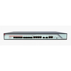
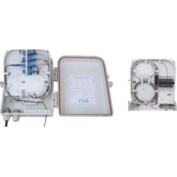
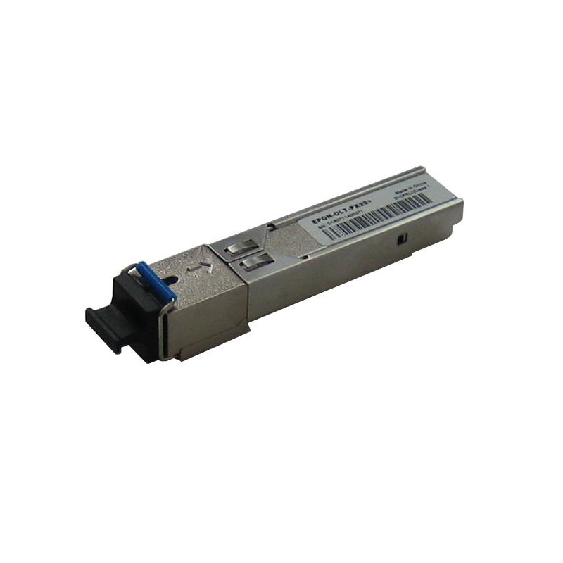
WDS5441H-C(H)3AL GEPON OLT SFP Transceiver modul, 1000BASE-PX20+, pro Wodaplug GEPON OLT jednotky
Základní popis
WDS5441H-C(H)3AL je velmi výkonný SFP transceiver optický modul pro single fiber komunikaci s vlnovou délkou 1490nm continuous-mode transmitter a 1310nm burst-mode receiver. Je navrľen dle standardů CTC 3.0 a IEEE802.3ah -2004 1000BASE- PX20+ pro EPON aplikace. Obousměrný symetrický datový přenos s rychlostí 1.25Gbps upstream and 1.25Gbps downstream na vzdálenost aľ 20km. Transmitter má automatickou kontrolu výkonu (Automatic power control APC) a teplotní cyrkulaci pro zajiątění stabilního optického výstupu a extinction ratia v celém pásmu provozních teplot. Transmitter splňuje Class 1 "eye safety" dle IEC825 a CDRH standardů. Receiver má hermeticky zapouzdřený APD-TIA (trans-impedance amplifier) předzesilovač a limitní zesilovač s LVPECL kompatibilním diferenciálním výstupem. Podporuje burst-mode Loss of signal (LOS) výstup a je LVTTL kompatibilní. Receiver má bust-mode RSSI výstup, který je I2C. Určeno pro jednotky Wodaplug WDS1U2PGE, 1U4PGE a 1U8PGE. General Description
WDS5441H-C(H)3AL is a high performance transceiver module for single fiber communications using a 1490nm continuous-mode transmitter and a 1310nm burst-mode receiver. It is designed to meet CTC 3.0 and IEEE802.3ah -2004 1000BASE- PX20+ applications. The transmitter has automatic power control (APC) function and temperature compensation circuitry to ensure stable optical power output and extinction ratio over all operating temperature range. The transmitter meets Class 1 eye safety per IEC825 and CDRH standards. The receiver has a hermetically packaged APD-TIA (trans-impedance amplifier) pre-amplifier and a limiting amplifier with LVPECL compatible differential outputs. It features a burst-mode Loss of signal (LOS) output which is LVTTL compatible. The receiver offers bust-mode RSSI outputs, which is I2C accessible digitized data stored in the internal flash memory.
Features
Applications
Standard
Absolute Maximum Ratings
Recommended Operating Conditions
Transmitter Optical and Electrical Characteristics
Note 1: Launched into 9/125um Single Mode Fiber. Note 2: Measured with PRBS 27-1 test pattern @1.25Gbit/s. Note 3: Measured with the Bessel-Thompson filter OFF. Note 4: Maximum sensitivity penalty due to transmitter and dispersion effect through 20km of SMF optical fiber. Note 5: Compatible with LVPECL input, AC coupled internally. Note 6: Transmitter enable and disable timing
Receiver Optical and Electrical Characteristics
Note 1: Measured with a PRBS 27-1 test pattern @1.25Gbit/s and ER=10dB, BER =10-12. Note 2: Input optical power level difference of adjacent burst packets. Note 3: Low level indicates that burst packet is detected by the receiver. Note 4: LVPECL output, DC coupled internally, guaranteed in the full range of input optical power (-6dBm to -30dBm) Note 5: RSSI DDM accuracy is better than +/-2dB (25℃) or +/-3dB (0℃~70℃) for input power levels between -6 to -30 dBm. Measured with 1310nm, 1.25Gbps PRBS27-1 burst-mode optical input, ER=10dB, 50%duty cycle. LOS Timing characteristicsThe Timing characteristics for RSSI
Figure 3 RSSI vs Trigger timing
Digital Diagnostic Monitor Accuracy
Pin Description
Note: TX Fault is an open collector/drain output, which should be pulled up with a 4.7K–10KΩ resistor on the host board. Pull up voltage between 2.0V to VccT+0.3V or VccR+0.3V. High output indicates a laser fault of some kinds. Low indicates normal operation. In the low state, the output voltage will be below 0.8V. TX disable is an input that is used to control the transmitter power output. It is pulled up within the module with a 4.7–10 KΩ resistor. Its states are: Low (0 – 0.8V): Transmitter on; (>0.8, < 2.0V): Undefined; High (2.0 – Vcc): Transmitter Disabled Open: Transmitter Disabled These pins should be pulled up with a 4.7K –10KΩ resistor on the host board. The pull-up voltage shall be VccT or VccR. Mod-Def 0 is grounded by the module to indicate that the module is present. RSSI TRIG is a LVTTL input. Assert high after 500ns delay time of the beginning of the monitored burst package,at least 500ns in duration. LOS (Loss of Signal) is an open collector/drain output, which should be pulled up with a 4.7K – 10KΩ resistor to VccT +0.3V or VccR+0.3V. Low level indicates that burst packet is detected by the receiver. RD-/+: These are the differential receiver outputs. They are DC coupled 100Ω differential line which should be terminated with 100Ω (differential) at the user SER.DES. VccR and VccT are the receiver and transmitter power supplies. They are defined as 3.3V ±5% at the SFP connector pin. Maximum supply current is 400mA. Recommended host board power supply filtering is shown interface circuit. Inductors with DC resistance of less than 1Ω, in order to insure the voltage at the SFP input pin with 3.3V. When the recommended supply filtering network is used, hot plugging of the SFP transceiver module will result in an inrush current of no more than 30 mA greater than the steady state value. VccR and VccT may be internally connected within the SFP transceiver module. TD-/+: These are the differential transmitter inputs. They are AC-coupled, differential lines with100Ω differential termination inside the module. The AC coupling is done inside the module and thus not required on the host board. |
|||||||||||||||||||||||||||||||||||||||||||||||||||||||||||||||||||||||||||||||||||||||||||||||||||||||||||||||||||||||||||||||||||||||||||||||||||||||||||||||||||||||||||||||||||||||||||||||||||||||||||||||||||||||||||||||||||||||||||||||||||||||||||||||||||||||||||||||||||||||||||||||||||||||||||||||||||||||||||||||||||||||||||||||||||||||||||||||||||||||||||||||||||||||||||||||||||||||||||||||||||||||||||||||||||||||||||||||||||||||||||||||||||||||||||||||||||||||||||||||||||||||||||||||||||

Mohlo by vás také zajímat